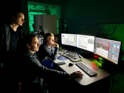
New high-resolution SEM/STEM instrument for multidimensional analysis of emerging nanomaterials installed at IMN/CENEM
IMN/CENEM is delighted to announce that a new high-resolution SEM/STEM instrument is enhancing the electron microscopy facility and expanding CENEM’s research capabilities.
The microscope, a GEMINI SEM 560 from Carl Zeiss Microscopy, was funded within the framework of a DFG proposal for major research instrumentation and was successfully installed last month at the Interdisciplinary Center for Nanostructured Films (IZNF). It is dedicated to high-resolution and multidimensional SEM/STEM analysis of emerging nanomaterials and accessible via CENEM’s user facility.
Application fields include, in particular, beam-sensitive and low-dimensional materials, in situ microscopy, as well as high-throughput and correlative workflows. The microscope is ideally suited for low-dose, low-kV, and reduced-pressure operation for high-resolution imaging, electron backscattered diffraction (EBSD), energy-dispersive X-ray spectroscopy (EDXS), and transmission diffraction (TD) analysis. Highlights are in particular an ultra-sensitive direct detection camera for EBSD (Clarity Super, Ametek) and a customized setup consisting of an ultrafast direct detection camera (Timepix 3) combined with a flexible hexapod sample stage (SmarAct) for TD. This dedicated equipment enables optimized crystal structure and orientation analysis of nanomaterials and beam-sensitive samples.
Key specifications:
- High-resolution electron column (Zeiss Gemini 3) featuring Schottky emission, low-kV optimized imaging and immersion-free optics (negligible magnetic field below objective lens), allowing imaging of magnetic materials (at WD = 3 mm; AV = 1 kV @ 100.000x magnification) without image distortions.
- Specified image resolutions:
- 0.4 nm at 30 kV (STEM).
- 0.5 nm at 15 kV (SEM).
- 0.8 nm at 1 kV (SEM).
- 1.0 nm at 0.5 kV (SEM).
- 1.0 nm at 1 kV (SEM-BSE Inlens detection).
- Optional sample biasing for best resolution conditions at low landing energies: 0.7 nm at 1 kV landing energy (SEM).
- Flexible and continuous tuning of acceleration voltage (0.02 – 30 kV) and beam current (3 pA – 20 nA).
- Detectors for multi-modal and high-resolution imaging: Everhart-Thornley SE-detector. High-resolution InLens SE detector. Energy-selective backscatter detector (EsB) with energy filter grid enabling pure BSE imaging. Retractable 6-segment BSE detector. Retractable 7-segment STEM detector. Cascade current detector for low-noise imaging during low vacuum operation. CCD cameras for sample navigation.
- Optional low vacuum operation (10 to 500 Pa). High resolution Inlens detectors can be used (in conjunction with beam sleeves) up to 150 Pa. Specified image resolutions:
- 1.4 nm at chamber pressure of 30 Pa and 3 kV.
- 1.0 nm at chamber pressure of 30 Pa and 15 kV.
- Direct detection EBSD camera (Clarity Super, Ametek GmbH) with excellent low-kV (~3 kV) and low dose (<10 pA) performance, zero read out noise and distortion, single-electron sensitivity and a high dynamic range.
- EDXS detector (Octane Elite Super, Ametek GmbH). Silicon drift detector with high sensitivity for detecting low energy signals (e.g. Al L at 73 eV) and high-resolution capability for both spatial and energy resolution (resolution at Mn Kα: 123 eV). Large detection area (70 mm²), fast electronics and high throughput count rate (limit: 850k output cps at 2.0m input cps). Carbon signal detection above 750k input cps. High-resolution quantitative analysis at mapping speeds greater than 400k output cps.
- Eucentric 6-axis sample stage.
- Automatic load lock (80 mm).
- In chamber plasma cleaner.
- Customized TD setup (under development):
- Hexapod stage (SmarAct GmbH) with eucentric tilt for precise and flexible sample positioning.
- Ultrafast direct detection camera (Timepix 3).
We highly appreciate the financial support from the DFG for this outstanding equipment.

